Research Projects
Projects
Atomic layer deposition (ALD) is a thin-film deposition technique that allows for the even growth of material over three-dimensional surfaces. It is especially useful because the growth occurs atomic layer by atomic layer in a self-limiting chemical reaction. This allows for the growth of ultrathin film with pristine quality and excellent conformity. We are utilizing this technique to fabricate novel supercapacitors by growing thin, high-k dielectric materials over patterned three-dimensional surfaces.
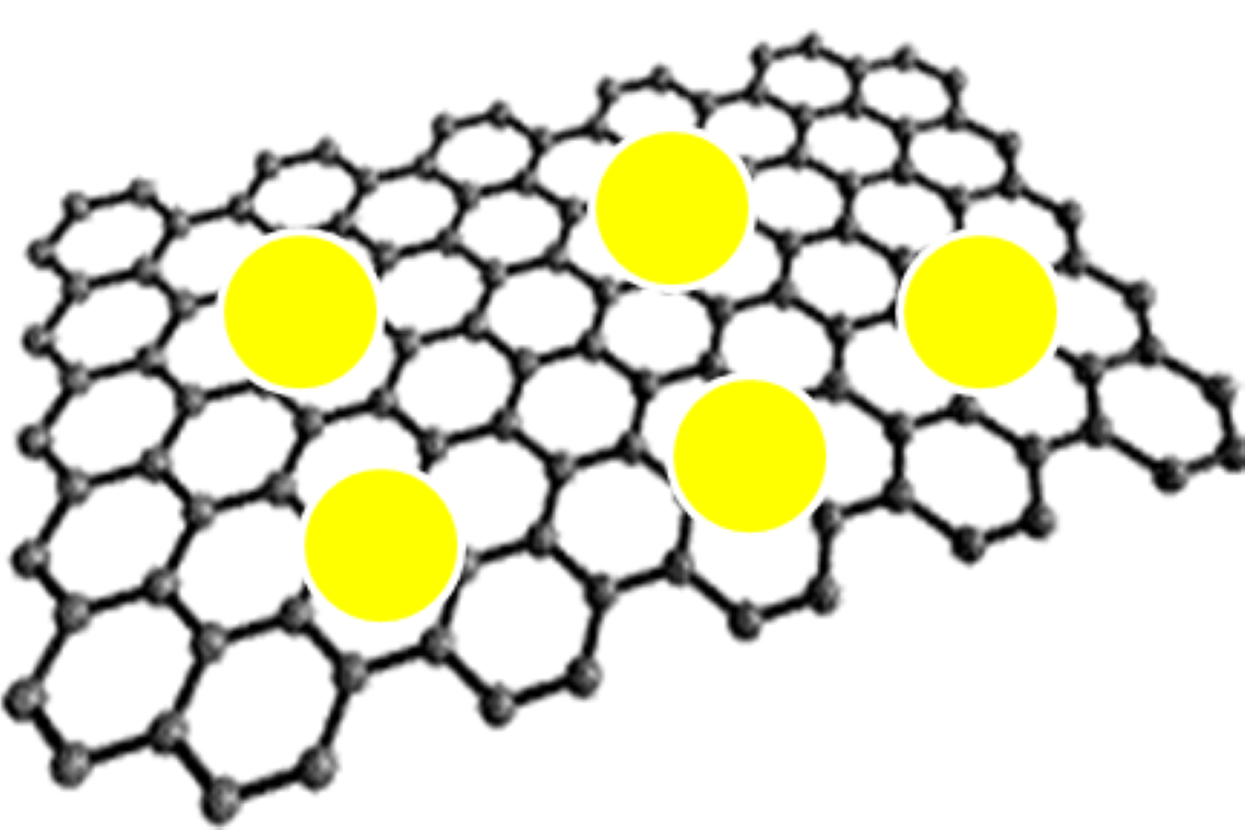
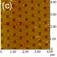
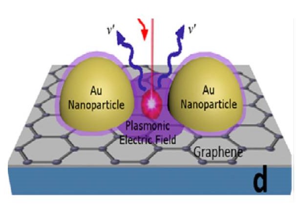
My research interest has been focused on the development of graphene transparent conductors and related electronic as well as optoelectronics devices, such as FET, and graphene photodetector. Most recently, we developed transparent conductors of graphene nanohole array (Figure 1) with tunable transmittance and conductance and plasmonic graphene (Figure 2) in which the surface plasmonic effect has been incorporated.
My current research involves improving carbon nanotube films for infrared detectors by manipulating the way that heat and charge carriers flow through the film. The film is made up of a lattice-like network of nanotubes and we are looking to improve the sensitivity of the detectors by improving the tube-to-tube contact and the film-to-substrate interface.
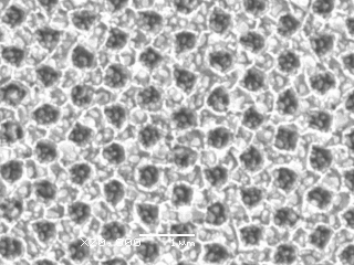
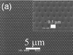
Nanopatterned 2D and 3D photonic crystal Fluorine-doped Tin Oxide (FTO) electrodes were created with nanoimprinting lithography. Au particles (~50-200 nm in diameter) formed on the nanopatterned FTO electrodes through evaporation followed by annealing. The morphology and particle size were characterized by SEM. The plasmonic effects were investigated via UV-Vis spectra transmission mode. Localized surface plasmon resonance position depends on the Au particles structure and size irrespective of the FTO pattern while transmittance relies on the pattern of FTO, Au particles structure, and size. The simulation predicts an enhanced scattering on such a structure.
Transparent conductors (TCs) are an important component of optoelectronic devices and nanoscale engineering of TCs is important for the optimization of the device performance. Despite being a commonly used TC in photovoltaic devices, fluorine-doped tin oxide (FTO) has limited transmittance in the solar spectrum. Improving the light transmittance and light scattering properties of FTO may lead to increased light absorption in the active volume of the photovoltaic device. In this work, patterned periodic arrays of nanopillars and nano lines of pitch size of ~700 nm were created on FTO using nanoimprint lithography and reactive ion etching using environmentally friendly gases. The patterned FTO photonic crystal exhibits enhanced light scattering as compared to the unpatterned FTO, which agrees well with simulations based on the Finite-Difference Time-Domain method. Dye-sensitized solar cells fabricated on the patterned FTO exhibited improved performance (fill factor and efficiency), which can be attributed to enhanced incident photon-to-current conversion in the range 400 - 650 nm as suggested also by theoretical simulations.
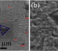
The major focus of my research has been on the fabrication of carbon-based nanomaterials for the application of energy conversion and storage devices. Recently, we have prepared graphene on a Cu substrate with various textures using chemical vapor deposition. Doped graphene nanohole arrays were fabricated for flexible transparent conductors, as shown in Figure 1. Also, we have developed an oxide-assisted self-assembly method for the growth of triangular graphene grains on cubic texture Cu substrates and the investigation of the growth mechanism of graphene, as shown in Figure 2. By engineering substrates, we can prepare graphene film with uniformity, high conductivity, and transparency.
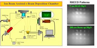
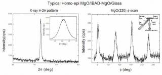
Ion beam-assisted deposition (IBAD) is widely used in developing textured templates on amorphous substrates in the last few years. It should be realized that the majority of thin films used for electronic and electrical devices need to be grown epitaxially, which normally requires a single crystal substrate with perfect lattice match and chemical compatibility. This has been a great limitation in practical applications. The IBAD texturing technique provides a novel approach for the epitaxy of thin films on nontextured substrates. IBAD-MgO has been successfully used to build texture on long metallic tapes for large-scale application of HTS YBCO-coated conductors. High-quality texture can be built within a few minutes on about 10 nm IBAD-MgO deposition. Homo-epitaxial MgO layer and other buffer layers can be used to further improve the epitaxy and surface compatibility with YBCO.
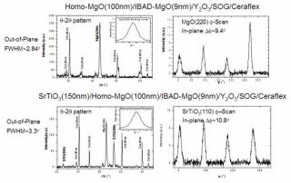
IBAD-MgO on non-metallic flexible Ceraflex. AC loss has been a serious concern of YBCO-coated conductor applications since most of HTS electrical devices need to work in a strong AC field. Non-metallic flexible Ceraflex is a possible candidate as a substrate to reduce AC loss of YBCO-coated conductors. It has very high resistivity so the eddy current loss will be totally removed; it also has excellent compatibility with YBCO since its composition is YSZ. It is flexible but the surface is very rough with Ra~100nm, which is not suitable for IBAD-MgO texturing. We used multi-layer Spin-on-Glass (SOG) to coat the original surface and reduce the Ra to about 1nm. A textured IBAD-MgO template has been developed on the SOG smoothened Ceraflex; then highly textured SrTiO3 film has been grown on top. A preliminary YBCO growth experiment on IBAD-MgO textured Ceraflex shows the phase is pure and the Tc is about 88K, optimization is still in progress.
IBAD-MgO on glass. Amorphous buffer layers are normally necessary for the IBAD-MgO texturing process. These buffer layers will induce additional loss and decrease efficiency. We tried to use Ar+ pre-bombarding to activate the substrate surface and obtained a highly textured IBAD-MgO template on unbuffered glass. By optimizing the pre-bombarding time, the best texture quality, in-plane ??~6.5o and out-of-plane FWHM~2o, has been obtained.
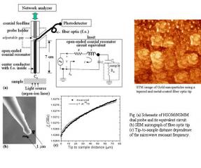
Correlation of different physical properties at microscopic to nanometer scales is crucial to understanding the basic physics in nano-matters. It should be realized that most existing SPM probes are single-channel and therefore can only image one physical property at a time. This motivated us to develop multi-channel SPM. The first microwave/optical dual-channel microprobe was demonstrated recently in our laboratory for simultaneous mapping of microwave and optical properties. The key element of this probe is the open-ended coaxial resonator terminated by a tapered and metal-coated fiber optic tip. Microwave is emitted/collected at the tip via the metal coating and light is emitted/collected via the core of the fiber. We extended the application of this metal-coated fiber tip to scanning tunneling microscopy (STM). Since the metal-coating (Gold) terminates at the tip apex but not covering the optical aperture, it facilitates the injection of tunneling electrons. With this probe, STM and near-field scanning optical microscopy (NSOM) experiments can be carried out. There is no doubt that these multi-channel SPM probes will become versatile tools for material research and nanoscience and we are currently carrying out some exciting applications.
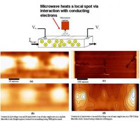
Imaging of different physical properties of a sample can also be realized by combining SPM techniques with macroscopic measurements. For example, we have integrated the microwave microprobe with electrical current-voltage (I-V) measurement. This allows us to excite the sample locally using the focused microwave from the probe and measure the sample voltage response. By recording this voltage response as a function of probe position, we can visualize the current flow pattern in a conductor. We can use this technique to map the current distribution in HTS-coated conductors and locate defects that impede the current flow. Moreover, other information about the sample area under investigation can be acquired. A microwave map reflecting the nonuniformity of structure and chemical composition through the HTS layer will reveal the location and form of defects. This method may provide a unique room-temperature technique for electrical current mapping in long-length HTS-coated conductors.
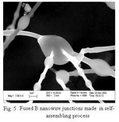
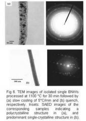
Nanoscale devices are promising for next-generation electronics. Our focus has been on exploring the controllable growth of nanowire arrays and studying their electrical transport properties. We are particularly interested in boron-based nanowires because of their unique and special characteristics. Single-crystal boron nanowires have been obtained from quenching the quartz tube in which a thermal vapor transfer method is used to deposit nanowires on Au-coated Si substrates. Furthermore, nanoscale Y-junctions and nano chains have been synthesized in our group.
The next step is to find out whether this light and high-temperature semiconductor can have high electrical conductivity in the nanowire or nanotube form as predicted by theoretical calculations. We are fabricating boron nanotubes and devising microscopic measurement procedures to verify this novel character.
Epitaxy and microstructure are important properties of high-temperature superconductors that directly impact their current carrying capabilities. For example, microstructural defects can improve supercurrent carrying capacity by providing normal state regions by which magnetic vortices are pinned. Because defects or non-superconducting regions in a type-II superconductor form energetically favorable penetration sites for magnetic vortices, an attractive force between the magnetic field line and the defect results, and the supercurrent impeding motion of vortices is dampened. Therefore, to improve the current carrying properties of materials such as YBa2Cu3Ox (YBCO), analysis and understanding of defect properties and mechanisms are crucial.
Since it is desirable that such defects are on the order of a coherence length (?ab ~ 2 nm in YBCO), transmission electron microscopy (TEM) is a valuable technique for the characterization of the microstructure. High-resolution TEM can characterize crystals to very small dimensions through both imaging and diffraction. TEM characterization of defects that are either intentionally inserted (such as nanoparticles) or those that result from other structural modifications (such as substrate-level surface modulations) gives direct evidence of their size and extent through the YBCO film and gives some understanding of the mechanisms responsible for interesting effects such as the porous films observed by our group.
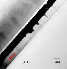
Another advantage of TEM characterization is that cross-sectional images can be obtained, thus showing the physical properties through the thickness of the film. For example, the image below shows a cross-section of a vicinal YBCO film on a miscut SrTiO3 substrate. Pores can be seen to extend through a significant portion of the film thickness. This illustrates an example of microstructurally modifying YBCO for the enhancement of its critical current.
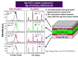
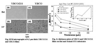
Coated conductor (see Fig. 4) research has been a central topic in the HTS research during the past few years. The so-called second-generation HTS tapes are expected to have tremendous potential for various electrical applications. One of the outstanding problems is the dramatic decrease of Jc with increasing HTS coating thickness. This problem must be solved for coated conductors to carry large currents. Our group has taken two approaches bottom-up by growing HTS films of different thicknesses and top-down by thinning them using ion milling to understand the physics related. We have also developed a new scheme for making porous HTS thick films to tailor the current flow. In collaboration with researchers at the Air Force research laboratory and Oak Ridge national laboratory, we have developed a microstructure-engineering scheme using vicinal growth induced strain plus Y2BaCuO5 nanoparticle insertion and achieved uniformly porous-structured YBCO thick films with much improved Jc.
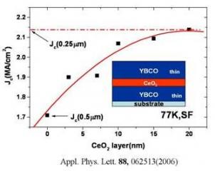
The relatively slowly decreasing Jc with the increasing thickness could be attributed to microstructure degradation for films thicker than 0.8 micrometers. However, the major Jc reduction happens in the thin film regime (film thickness less than 0.8~1.0 micrometers), where the microstructure degradation is not a concern. Our approach to addressing this issue is to apply the multilayer structure in which thick YBCO films are evenly chopped into thin films with insulating spacers. The experiment result on a trilayer YBCO/CeO2/YBCO, where a 0.5-micrometers-thick YBCO layer was divided into two 0.25-micrometers-thick YBCO layers by a thin insulator layer of CeO2, shows that the Jc increases with the thickness of CeO2. This observation suggests that, by gradually decoupling the fluxons in two adjacent YBCO layers, the thin film pinning efficiency is achieved which is in line with the 2D collective pinning model.
High critical current density (Jc) is the most critical specification for high-temperature superconductor-coated conductors as required by numerous electric power-related applications. This has motivated an intensive research effort on the effects of microstructure on Jc. By growing YBa2Cu3O7-? (YBCO) films at a small vicinal angle we have recently obtained a highly porous structure in these films accompanied by a significantly enhanced Jc and smaller Jc reduction at larger film thickness. Furthermore, we tailored the porosity by inserting Y2BaCuO5 (211) nanoparticles in vicinal YBCO thick films to alter the strain at the nanometer scale. A nearly doubled pore density was obtained. A further improved Jc as the consequence of the enhanced pore density in these films suggests a direct correlation between microstructure and Jc and projects an even higher Jc in YBCO films with microstructure engineered optimally at a nanometer scale
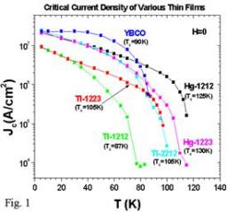
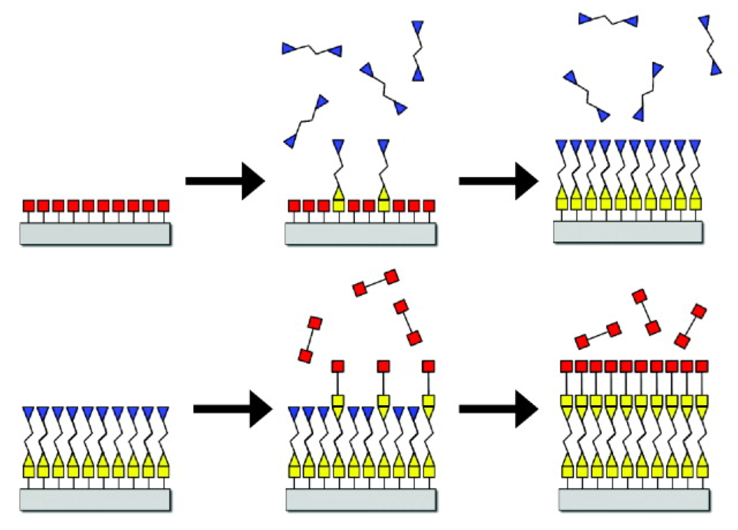
The discovery of the first high-temperature superconductor (HTS) by Bednoz and Miller in 1986, which won them the Nobel prize, triggered a worldwide effort in HTS research because of the tremendous potential of these materials in applications. Among many other HTSs, Hg-based HTS (HgBa2Can-1CunO2n+2, n=1,2,3,4), or Hg-HTSs, have the highest superconducting transition temperature Tc of 135 K. The highly volatile nature of the Hg-based compounds, however, makes the epitaxy of Hg-HTS films the toughest challenge so far in the HTS material research. We have developed several new processes including an alkaline doping-assisted process to promote liquid phase formation which accelerates the formation of the Hg-HTS phase, and a fast temperature ramping process to bring the processing temperature directly to the window so as to minimize the formation of the impurity phases. Using these new processes, we have demonstrated high-quality Hg-1223 films with Tc>130K and followed with many interesting studies on these films.
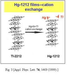
Despite the many exciting results on Hg-HTS films that her group achieved early on, two problems hindered further progress: poor run-to-run reproducibility and severe film/substrate reaction. These generic problems associated with the epitaxy of volatile compounds in conventional material processing prompted us to invent a non-conventional cation exchange process. This process employs a precursor matrix of similar crystalline structure and chemical composition to the desired material but without volatile cations such as Hg. By providing perturbations to the guest cations on the sites near the final sites of the volatile cations, the guest cations can be replaced with volatile cations without collapsing the crystal structure, like an atomic surgery over an existing crystal lattice. The microscopic mechanism of the cation exchange has been a focus of our group in recent years and the question we would like to answer is how it occurs at a microscopic scale, what are the relevant processing parameters, and whether it can be applied to design a new material using existing ones.
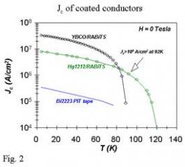
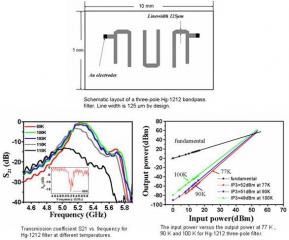
The increased research interest in the microwave applications of high-temperature superconductors (HTS) was brought about by the perceived potential of the marketability of superconducting electronics, especially in the wireless communications industry. Excellent surface morphology and high reproducibility of the HgBa2CaCu2O6+d (Hg-1212) thin films made from the cation exchange process have motivated us to develop microwave bandpass filters, which can be operated at above 77 K and therefore are much more cost-effective. High-quality Hg-1212 three-pole filters have been successfully fabricated. The filters exhibited lower insertion loss even at higher operating temperatures, compared with bandpass filters made of YBCO and copper with the same mask. The power handling capability of the filter was characterized by monitoring the third-order intermodulation signals. The power scaling of IM3 products in the Hg-1212 filter with regard to input power was around 2.8:1, well consistent with theoretically predicted scaling: 3:1. The IP3 of the Hg-1212 filter was 51 dBm at 90K, which was comparable to that of YBCO at 77K. This improved performance was attributed mainly to its higher Tc, which makes Hg-1212 a promising alternative material for passive microwave devices.
Bibek Gautam, Mary Ann Sebastian, Shihong Chen, Jack Shi, Timothy Haugan, Zhongwen Xing, Wenrui Zhang, Jijie Huang, Haiyan Wang, Mike Osofsky, Joseph Prestigiacomo, and Judy Z. Wu AIP Advances 7, 075308 (2017); doi:http://dx.doi.org/10.1063/1.4991051
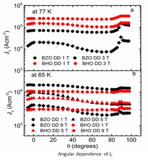
An elastic strain model was applied to evaluate the rigidity of the c-axis aligned one-dimensional artificial pinning centers (1D-APCs) in YBa 2 Cu 3 O 7-δ matrix films. Higher rigidity was predicted for BaZrO 3 1D-APCs than that of the BaHfO 3 1D-APCs. This suggests a secondary APC doping of Y 2 O 3 in the 1D-APC/YBa 2 Cu 3 O 7-δ nanocomposite films would generate a stronger perturbation to the c-axis alignment of the BaHfO 3 1D-APCs and therefore a more isotropic magnetic vortex pinning landscape. In order to experimentally confirm this, we have made a comparative study of the critical current density J c (H, θ, T) of 2 vol.% BaZrO 3 + 3 vol.%Y 2 O 3 and 2 vol.%BaHfO 3 + 3 vol.%Y 2 O 3 double-doped (DD) YBa 2 Cu 3 O 7-δ films deposited at their optimal growth conditions. A much enhanced isotropic pinning was observed in the BaHfO 3 DD samples. For example, at 65 K and 9.0 T, the variation of the J c across the entire θ range from θ=0 (H//c) to θ=90 degree (H//ab) is less than 18% for BaHfO 3 DD films, in contrast to about 100% for the BaZrO 3 DD counterpart. In addition, lower α values from the J c (H) ∼ H -α fitting were observed in the BaHfO 3 DD films in a large θ range away from the H//c-axis. Since the two samples have comparable J c values at H//c-axis, the improved isotropic pinning in BaHfO 3 DD films confirms the theoretically predicted higher tunability of the BaHfO 3 1D- APCs in APC/YBa 2 Cu 3 O 7-δ nanocomposite films.
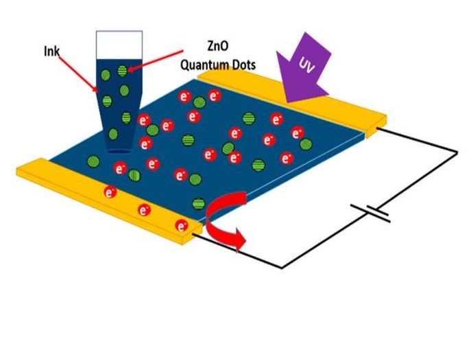
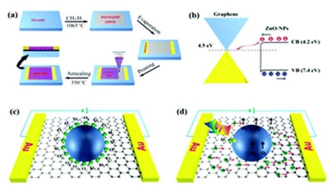
A nanocomposite ink composed of zinc oxide precursor (ZnOPr) and crystalline ZnO quantum dots (ZnOPrQDs) has been explored for printing high-performance ultraviolet (UV) photodetectors. The performance of the devices has been compared with their counterparts printed from ZnOPr ink without ZnO QDs. Remarkably, higher UV photoresponsivity of 383.6 A/W and the on/off ratio of 2470 is observed in the former, which are significantly better than 14.7 A/W and 949 in the latter. The improved performance is attributed to the increased viscosity in the nanocomposite ink to enable a nonporous structure with improved crystallinity and surface-to-volume ratio. This is key to enhanced surface electron-depletion effect for higher UV responsivity and on/off ratio. In addition, QD-assisted printing provides a simple and robust method for printing high-performance optoelectronics and sensors.
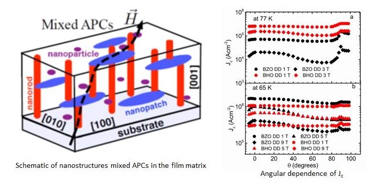
An elastic strain model was applied to evaluate the rigidity of the c-axis aligned one-dimensional artificial pinning centers (1D-APCs) in YBa2Cu3O7-δ matrix films. Higher rigidity was predicted for BaZrO3 1D-APCs than that of the BaHfO3 1D-APCs. This suggests a secondary APC doping of Y2O3 in the 1D-APC/YBa2Cu3O7-δ nanocomposite films would generate a stronger perturbation to the c-axis alignment of the BaHfO3 1D-APCs and therefore a more isotropic magnetic vortex pinning landscape. In order to experimentally confirm this, we have made a comparative study of the critical current density Jc (H, θ, T) of 2 vol.% BaZrO3 + 3 vol.%Y2O3 and 2 vol.%BaHfO3 + 3 vol.%Y2O3 double-doped (DD) YBa2Cu3O7-δ films deposited at their optimal growth conditions. A much enhanced isotropic pinning was observed in the BaHfO3 DD samples. For example, at 65 K and 9.0 T, the variation of the Jc across the entire θ range from θ=0 (H//c) to θ=90 degree (H//ab) is less than 18% for BaHfO3 DD films, in contrast to about 100% for the BaZrO3 DD counterpart. In addition, lower α values from the Jc(H) ∼ H-α fitting were observed in the BaHfO3 DD films in a large θ range away from the H//c-axis. Since the two samples have comparable Jc values at H//c-axis, the improved isotropic pinning in BaHfO3 DD films confirms the theoretically predicted higher tunability of the BaHfO3 1D-APCs in APC/YBa2Cu3O7-δ nanocomposite films.
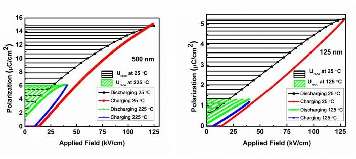
The influence of temperature on the energy storage behavior of relaxor-ferroelectric epitaxial Pb0.92La0.08Zr0.52Ti0.48O3 (PLZT) thin film capacitors fabricated using pulsed laser deposition was evaluated using cyclic I-V measurements from 25 °C to 225 °C in order to elucidate ferroelectric and dielectric contributions across the Curie temperature. In the film thickness range of 125 nm to 500 nm, it has been found that the leakage current through the capacitors increases monotonically with increasing temperature, and the effect are more prominent at smaller film thickness, primarily due to a more efficient movement of ferroelectric domains. While these effects prevent thinner PLZT films from maintaining adequate energy storage efficiencies at temperatures above~ 100 °C, thicker films show promising energy storage properties in a wide temperature range. Specifically, the 500 nm thick PLZT film capacitors have a nearly constant energy storage efficiency above ~70% in the temperature range of 25 °C to 175 °C, with a peak efficiency of 78% at 175 °C due to the large dielectric constant exceeding ~2000 as the temperature approaches the PLZT Curie temperature of 200 °C. By quantifying the three contributions of the electric conductivity, dielectric capacitance, and relaxor-ferroelectric domain switching polarization to temperature-dependent energy storage properties of relaxor-ferroelectric capacitors, this study reveals that the dielectric contribution dominates in the PLZT capacitors with smaller thickness, while even contributions from all three components are present in films of larger thickness. These results suggest that the PLZT relaxor-ferroelectric thin film capacitors are promising for energy storage applications and further improvement of performance may be achieved by optimization of the film/electrode interface.
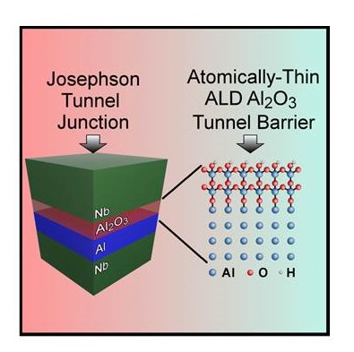
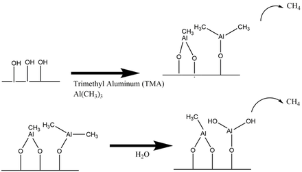
Atomic Layer Deposition (ALD) is a promising technique for the production of ultrathin, low-defect-density tunnel barriers for metal-insulator-metal tunnel junctions (MIMTJs). A fundamental challenge lies with the atomic scale control of the M-I interface. Using an Al wetting layer with a controlled H2O surface activation, Nb/Al/Al2O3/Nb Josephson junctions (JJs) were fabricated in situ with ALD-Al2O3 tunnel barriers ranging from 0.1 – 1.2 nm in thickness. In situ Scanning Tunneling Spectroscopy was utilized to compare the ALD-Al2O3 tunnel barriers against traditional thermal AlOx tunnel barriers formed via oxygen diffusion. Fundamental differences in tunnel spectra characteristics, barrier height, and breakdown behavior were observed. Remarkably, the tunnel barrier height of the former was found to be significantly higher than the latter. This property was corroborated by the JJ’s I-V characteristics at cryogenic temperatures. Together, these measurements suggest that ALD-Al2O3 is a substantially denser, less defective, and leak-free ultrathin tunnel barrier for high-performance MIMTJs.
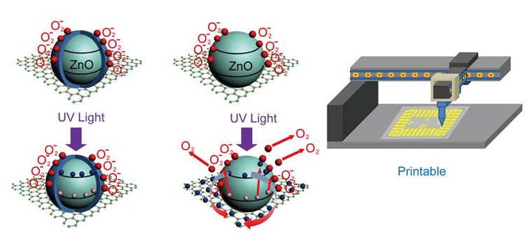
In ZnO quantum dot/graphene heterojunction photodetectors, fabricated by printing quantum dots (QDs) directly on the graphene field-effect transistor (GFET) channel, the combination of the strong quantum confinement in ZnO QDs and the high charge mobility in graphene allows extraordinary quantum efficiency (or photoconductive gain) in visible-blind ultraviolet (UV) detection. Key to the high performance is a clean van der Waals interface to facilitate an efficient charge transfer from ZnO QDs to graphene upon UV illumination. Here, we report a robust ZnO QD surface activation process and demonstrate that a transition from zero to extraordinarily high photoresponsivity of 9.9 × 10⁸ A/W and a photoconductive gain of 3.6 × 10⁹ can be obtained in ZnO QDs/GFET heterojunction photodetectors, as the ZnO QDs surface is systematically engineered using this process. The high figure-of-merit UV detectivity D* in exceeding 1 × 10¹⁴Jones represents more than 1 order of magnitude improvement over the best reported previously on ZnO nanostructure-based UV detectors. This result not only sheds light on the critical role of the van der Waals interface in affecting the optoelectronic process in ZnO QDs/GFET heterojunction photodetectors but also demonstrates the viability of printing quantum devices of high performance and low cost.
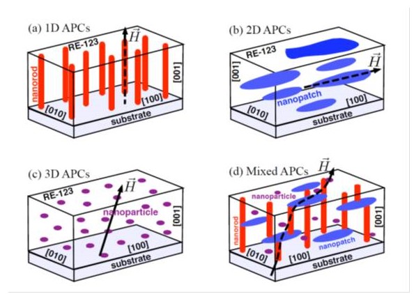
Raising critical current density J c in high-temperature superconductors (HTSs) is an important strategy towards performance-cost balanced HTS technology for commercialization. The development of strong nanoscale artificial pinning centers (APCs) in HTS, such as YBa2Cu3O7 or RE-123 in general, represents one of the most exciting progressions in HTS material research in the last decade. Significantly raised J c has been demonstrated in APC/RE-123 nanocomposites by enhanced pinning on magnetic vortices in magnetic fields towards that demanded in practical applications. Among other processes, strain-mediated self-organization has been explored extensively for in situ formation of the APCs based on fundamental physics design rules. The desire in controlling the morphology, dimension, orientation, and concentration of APCs has led to a fundamental question on how strains interact in determining APCs at a macroscopic scale. Answering this question demands an interactive modeling-synthesis-characterization approach toward a thorough understanding of fundamental physics governing the strain-mediated self-organization of the APCs in the APC/RE-123 nanocomposites. Such an understanding is the key to a leap forward from the traditionally empirical method to materials-by-design to enable an optimal APC landscape to be achieved in epitaxial films of APC/YBCO nanocomposites under the precise guidance of fundamental physics. The paper intends to provide a review of recent progress made in the controllable generation of APCs using the interactive modeling-synthesis-characterization approach. The emphasis will be given to the understanding so far achieved using such an approach on the collective effect of the strain field on the morphology, dimension, and orientation of APCs in epitaxial APC/RE-123 nanocomposite films.
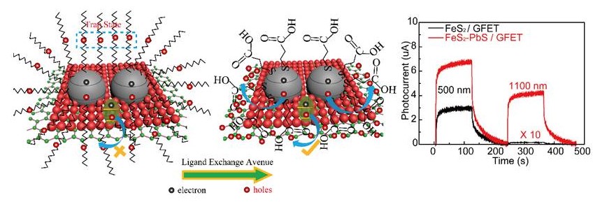
Colloidal nanocrystals are attractive materials for optoelectronics applications because they offer a compelling combination of low-cost solution processing, printability, and spectral tunability through the quantum dot size effect. Here we explore a novel nanocomposite photosensitizer consisting of colloidal nanocrystals of FeS2 and PbS with complementary optical and microstructural properties for broadband photodetection. Using a newly developed ligand exchange to achieve high-efficiency charge transfer across the nanocomposite FeS2-PbS sensitizer and graphene on the FeS2-PbS/graphene photoconductors, an extraordinary photoresponsivity exceeding ~106 A/W was obtained in an ultrabroad spectrum of ultraviolet (UV)-visible-near infrared (NIR). This is in contrast to the nearly three orders of magnitude reduction of the photoresponsivity from~106 A/W at UV to 103 A/W at NIR on their counterpart of FeS2/graphene detectors. This illustrates the combined advantages of the nanocomposite sensitizers and the high charge mobility in FeS2-PbS/graphene van der Waals heterostructures for nanohybrid optoelectronics with high performance, low cost, and scalability for commercialization.
Combining the high mobility of graphene and the surface electron depletion effect of zinc oxide nanoparticles (ZnO-NPs), graphene/ZnO-NP nanohybrids can be anticipated for significantly enhanced photoresponsivity and photoconductive gain in optoelectronics. Herein, a transfer-free and printable method was developed for the fabrication of wafer-size graphene/ZnO-NP nanohybrids for high-performance UV photodetectors. These photodetectors achieved the extraordinary photoresponsivity of up to 1000 A W (1) V (1) and a high gain of 1.8 x 10(4), representing more than an order of magnitude improvement compared to that of previously reported UV photodetectors based on various ZnO nanostructures and transferred-graphene/ZnO nanohybrids. Our method provides a low-cost pathway for the run-to-run wafer-size fabrication of high-performance graphene/ZnO optoelectronics.
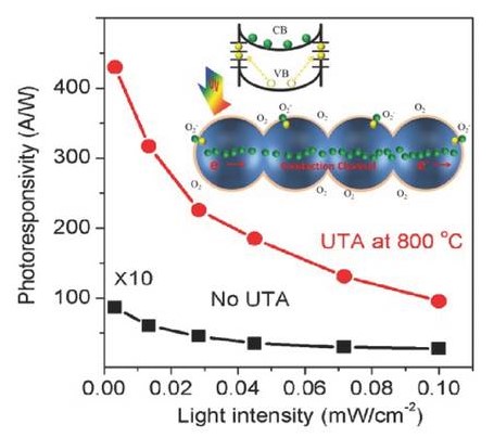
Zinc oxide nanoparticles (ZnO-NPs) with a radius of the Debye length have the optimal electron depletion effect for high-performance optoelectronic devices. However, a major challenge remains in assembling ZnO-NPs into 3D interlinked networks for high-efficiency electron transport. Here an ultrafast thermal annealing process has been developed by exposing the ZnO-NPs to excessive heat for a short period of 2 s. This enables the formation of NP-NP interface nanojunctions, resulting in nearly two orders of magnitude decrease of the dark current I-Dark and more than an order of magnitude increase of the photocurrent I-Ph under ultraviolet (UV) illumination. Moreover, the UV photodetectors based on such 3D interlinked ZnO-NP networks exhibit extraordinary performance with a high I-Ph/I-Dark ratio of 3.1 x 10(5), the responsivity of up to 95.4 A W-1 at 340 nm UV power of 0.1 mW cm(-2) (and up to 430 A W-1 at 0.003 mW cm(-2)), detectivity of 1.4 x 10(13) Jones, and rise/decay time of 9.4 s/13.5 s. These results illustrate the critical importance of the NP-NP interface nanojunctions and provide a low-cost pathway for high-performance ZnO-NP optoelectronics.
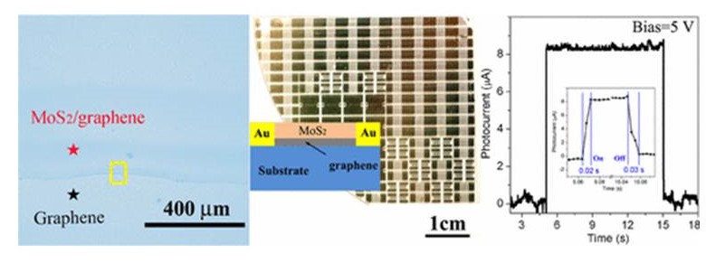
Two-dimensional (2D) MoS2/graphene van der Waals heterostructures integrate the superior light solid interaction in MoS2 and charge mobility in graphene for high-performance optoelectronic devices. The key to the device's performance lies in a clean MoS2/graphene interface to facilitate the efficient transfer of photogenerated charges. Here, we report a printable and transfer-free process for the fabrication of wafer-size MoS2/graphene van der Waals heterostructures obtained using a metal-free grown graphene, followed by low-temperature growth of MoS2 from the printed thin film of ammonium thiomolybdate on graphene. The photodetectors based on the transfer-free MoS2/graphene heterostructures exhibit extraordinarily short photoresponse rise/decay times of 20/30 ms, which are significantly faster than those of the previously reported MoS2/transferred-graphene photodetectors (0.28-1.5 s). In addition, a high photoresponsivity of up to 835 mA/W was observed in the visible spectrum on such transfer-free MoS2/graphene heterostructures, which is much higher than that of the reported photodetectors based on the exfoliated layered MoS2 (0.42 mA/W), the graphene (6.1 mA/W), and transfer-free MoS2/graphene/SiC heterostructures (similar to 40 mA/W). The enhanced performance is attributed to the clean interface on the transfer-free MoS2/graphene heterostructures. This printable and transfer-free process paves the way for large-scale commercial applications of the emerging 2D heterostructures in optoelectronics and sensors.
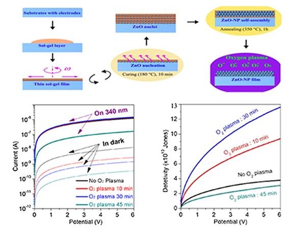
Zinc oxide (ZnO) nanoparticles (NPs) with uniform particle radius comparable to the desired Debye length provide a low-cost and scalable scheme to achieve an optimized electron depletion effect, which is the key to high-performance ultraviolet (UV) photodetection. Here, a simple and improved sol–gel method for in situ synthesis of highly crystalline constituent ZnO-NP mesoporous thin films is reported. In combination with optimal oxygen plasma treatment to activate the ZnO-NP surface, the UV-detection performance is enhanced remarkably with a reduced dark current by one order of magnitude and an increased UV detectivity by over 300%. Moreover, such UV photodetectors exhibit extraordinary performance with a high responsivity of up to 0.8 A W−1V−1 at 340 nm UV power of 0.003 mW cm−2, detectivity of 1.4 × 10¹¹ Jones, and rise/decay time of 3.4 s/5.0 s. These results illustrate that the sol–gel ZnO-NP films provide a promising template for high-performance UV detectors to take full advantage of the electron depletion effect.
A novel type of substrate for quantitative surface-enhanced Raman spectroscopy (SERS) composed of chemical vapor deposition (CVD) graphene and in-situ fabricated rounded gold nanoparticles (AuNPs) was designed. SERS was measured on samples of different concentrations of Rhodamine 6G (R6G) on the AuNPs/graphene substrates using a low-power 632.8 nm laser. Finite element simulations were carried out for a system of two gold hemiellipsoids under various conditions such as with an R6G analyte covering the surface and with graphene underneath the nanoparticles. Graphene or R6G being present between the two nanoparticles caused a redshift in the plasmonic resonance frequency, and the graphene dampened the electric field of the surface. Regardless of the weakened electric field, the synergy of the AuNPs and graphene still enhanced the Raman signature of R6G to a greater extent than the nanoparticles or graphene alone could, which is attributed to the charge-transferring mechanism effect of graphene on SERS. The lowest concentration of solid phase R6G deposited in this manner that could be detected was 8 107 M. Higher analyte concentrations and the characteristic peak intensities of the analyte showed a logarithmic relation as anticipated from the plasmonically enhanced Raman scattering.
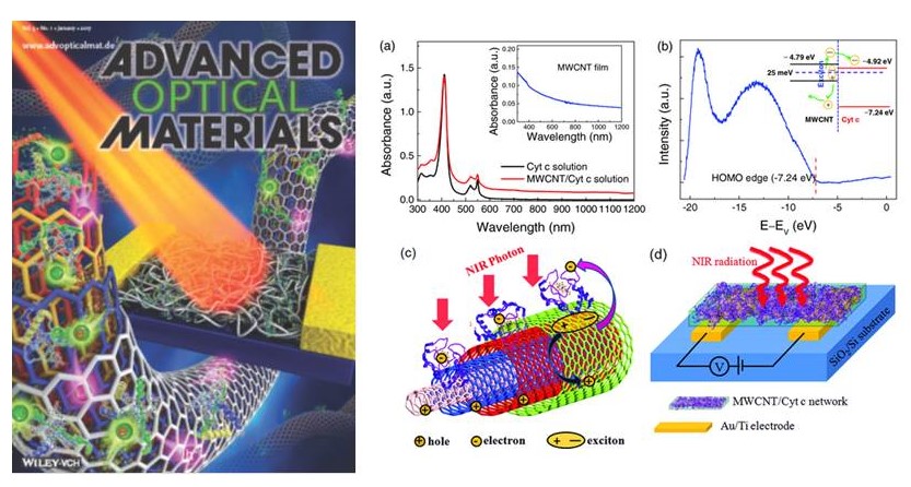
A novel MWCNT/Cyt c heterojunction nanohybrid uncooled IR photodetector has been demonstrated. The high-effective exciton dissociation derived from the heterojunction at the interface between MWCNT (donor) and Cyt c (acceptor) results in a remarkable NIR responsivity up to ≈0.30 A W−1 at room temperature. This value represents one to three orders of magnitudes improvement over that reported on CNT-only NIR detectors and is attributed to the critical role of the interface heterojunctions in assisting exciton dissociation to photocurrent and combination of efficient charge transport of CNT (holes) and Cyt c (electrons). Consequently, a high EQE up to 38.2% has been achieved on MWCNT/Cyt c heterojunction nanohybrid uncooled IR photodetectors, which represents a significant improvement by two orders of magnitude over the MWCNT-only IR detectors. In addition to the high detectivity of 1.8 × 10⁷ jones and fast photoresponse with response times of 1.5–2.7 ms, this result opens up a new potential direction through nanoscale interface design for exploration of high performance, low cost, and flexible carbon-based optoelectronic nanohybrid
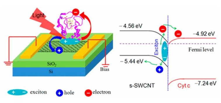
Inorganic/biomolecule nanohybrids can combine superior electronic and optical properties of inorganic nanostructures and biomolecules for optoelectronics with performance far surpassing that achievable in conventional materials. The key to a high-performance inorganic/biomolecule nanohybrid is to design its interface based on the electronic structures of the constituents. A major challenge is the lack of knowledge of most biomolecules due to their complex structures and composition. Here, we first calculated the electronic structure and optical properties of one of the cytochrome c (Cyt c) macromolecules (PDB ID: 1HRC) using ab initio OLCAO method, which was followed by experimental confirmation using ultraviolet photoemission spectroscopy. For the first time, the highest occupied molecular orbital and lowest unoccupied molecular orbital energy levels of Cyt c, a well-known electron transport chain in biological systems, were obtained. On the basis of the result, pairing the Cyt c with semiconductor single-wall carbon nanotubes (s-SWCNT) was predicted to have a favorable band alignment and built-in electrical field for exciton dissociation and charge transfer across the s-SWCNT/Cyt c heterojunction interface. Excitingly, photodetectors based on the s-SWCNT/Cyt c heterojunction nanohybrids demonstrated extraordinary ultra-broadband (visible light to infrared) responsivity (46–188 A W–1) and figure-of-merit detectivity D* (1–6 × 1010 cm Hz1/2 W–1). Moreover, these devices can be fabricated on transparent flexible substrates by a low-lost nonvacuum method and are stable in the air. These results suggest that the s-SWCNT/biomolecule nanohybrids may be promising for the development of CNT-based ultra-broadband photodetectors.
Flexible Quantum Dot/Graphene Nanohybrid Photodetectors
Colloidal quantum dots (QDs)/graphene nanohybrid heterostructures provide a promising scheme for quantum sensors as they take advantage of the strong quantum confinement in QDs with enhanced light-matter interaction, spectral tunability, suppressed phonon scattering, and extraordinary charge mobility in graphene at room temperature. We have developed a flexible 9-channel PbS QDs/graphene nanohybrid imaging array on polyethylene terephthalate and demonstrated imaging at broadband wavelengths in the ultraviolet-visible-near infrared range.
