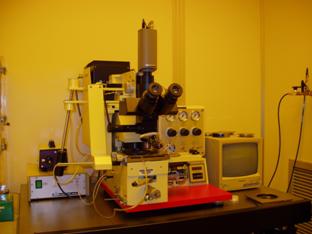
Mask Aligner with UV Exposure for Photolithography
This system facilitates transfer of circuit and device designs onto a thin film sample or wafer by exposing parts of the polymer-covered sample/wafer to ultraviolet radiation using a photolithographic mask pattern. This process is a precursor to chemical wet etching, ion beam milling or reactive ion etching.
Picture:

Equipment type:
Preparation and Fabrication